The process by which the different components required to construct an electronic circuit are positioned on the PCB, prepared for the subsequent welding phase, is known as the assembly phase of a printed circuit, often known by the abbreviation PCBA (Printed Circuit Board Assembly). Therefore, PCBA is one of the several phases that make up the fabrication of a printed circuit. As such, it offers certain important problems, mostly those that relate to the components, which will now be thoroughly examined.
Assembly methods
The methods needed for PCB construction have changed as electronic technology have advanced quickly through time. In general, there are two basic methods for assembling printed circuit boards, and a third, formed by combining the first two, is added.
The surface mount
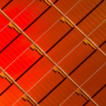
This technology, sometimes referred to as SMT (Surface Mount Technology), involves attaching surface mount devices (SMD) to the printed circuit board. Due to their relatively tiny standard packaging, SMD components are especially sensitive and important during the assembly phase (positioning and temperature reached during soldering must be carefully controlled). In today’s surface assembly equipment, completely automated processes (such pick and place) are used to pick up and precisely put each component on the PCB. A SMD component can have dimensions even smaller than the tip of a pencil, as is the case with the 01005 package (see Figure 1).

Through-hole construction
Thru-Hole Technology, often known as THT, is the name used to describe the PCB assembly method that has been utilised for years. It applies to parts with two or more terminals that were manufactured to fit through the PCB’s holes during production, such as capacitors, coils, transformers, high resistances, and inductances. On the side where the terminals protrude, welding is carried out. Through-hole mounting enables assembly of even extremely big components, whereas SMT technology is better suited to tiny components.
A hybrid technology
The most recent generation of electronic circuits have a high level of complexity due to the integration of numerous components in an ever-shrinking area. With the increasing usage of SMT and THT technologies during the assembly phase, it is not always possible to run a PCBA with only one type of component (SMD or PTH). These technologies must be appropriately calibrated and sequenced in to make the assembly and subsequent welding easier.
Importance of the constituents
The majority of the time, one or more components are to blame for a board’s problems. Therefore, it’s crucial to identify the key significant components and their potential to malfunction in order to produce an assembly that is rapid and error-free.
Moisture
Electronic components manufactured on PCBs are greatly threatened by moisture. It can be created both during the component’s manufacture and throughout the several stages of the board’s building. Additionally, condensation can happen to the printed circuit and the components attached to it. This is often caused when the boards are stored in containers with a lower temperature than the surrounding air. Therefore, while choosing the components themselves, it is important to carefully consider some components’ high sensitivity to dampness.
Temperature
PCBs must perform in harsh environmental conditions in the industrial, automotive, and transportation sectors, where temperature, pressure, and corrosion can affect how well-designed parts and circuits function. While keeping in mind that in many situations, the extended temperature range is required, it is always important to carefully evaluate the effects that temperature has on a system. This requires choosing sturdy components and implementing suitable thermal management techniques, either active or passive, that are intended to keep the operating temperatures of the components within a reasonable range.
Peaks in voltage and current
The most delicate parts that are not adequately protected from voltage and current spikes caused by power supply lines, design flaws, component deterioration, or (in the case of high power circuits) by the development of actual electric arcs might be irrevocably damaged.
Radiation
The majority of radiation-related issues are restricted to reducing the impacts of electromagnetic radiation (EMI). This factor is crucial because, if ignored, it can cause signal integrity issues that make it impossible to reliably transmit a high-speed signal between two locations in the circuit. The impact of radiation on electronic components can result in serious harm for PCBs mounted aboard spacecraft, where great dependability is required.
Mechanical tensions
The assembly of PCBs for industrial, aerospace, and automotive (to name the three main industries) applications must adequately account the factors relating to mechanical stress. These include shocks and vibrations that not only cause partial separation of the heaviest or most mechanically sensitive components, but also bend or shatter the printed circuit board.
Span of time
Due to the quick development of electronic technology, components have a certain lifespan after which they become “end of life,” as the term is used (EOL). You greatly raise the risk of failure or malfunction caused by wear and physical or mechanical stress if you overlook this element and keep using components in your designs that are in the EOL condition. The components in EOL will likely not be able to fulfil the increased performance criteria, operating with wider margins of error and a higher chance of failure since they have been surpassed by new technical developments and are no longer upgraded.
Some assembly advice
After examining the effects of a few crucial component-related difficulties on the assembly, we will now discuss some sound design principles that can streamline and enhance the PCBA’s overall quality.
1 – Using a variety of technologies
As a general rule, mixed assembly technologies should only be used in certain circumstances. For instance, the cost and effort added for assembly virtually never outweigh the benefit of inserting a single through hole (PTH) component. Instead, using numerous PTH components or excluding them entirely from the design is preferred and more effective. It is advised to arrange all through-hole components on the same face of the printed circuit if PTH technology is required. This will speed up assembly.
2 – Component size
It’s crucial to choose the appropriate package size for each component during the PCB design process. In general, larger packages should be chosen instead of smaller ones unless there is a good reason to do so. In reality, electrical designers frequently choose parts with excessively tiny packaging, which might lead to issues during the assembly process and even the need to modify the circuit. Depending on the degree of the modification required, it may be more practical to reassemble a board entirely than to disassemble it and solder the necessary components.
3 – Footprint of a component
Another crucial component of assembly is component footprint. As a result, the PCB designer must make sure that each footprint is appropriately built using the land pattern described in each integrated component’s datasheet. The development of the so-called “tombstoning,” often referred to as the Manhattan effect or the crocodile effect, is the principal issue brought on by an erroneous footprint. When an integrated component is soldered, this issue arises when an unequal amount of heat is delivered to it, causing it to adhere to the PCB just on one side rather than both. Tombstoning, which mostly affects passive SMD components like resistors, capacitors, and inductors, is brought on by uneven heating as a result of:
- Inadequate component-related land pattern dimensions;
- exceptionally large track width, which serves as a heat sink;
- various amplitudes of the tracks linked to the component’s two pads.
4 – Space between components
Overheating brought on by inadequate air space between components is one of the primary reasons of PCB malfunction. Space is a valuable resource, particularly when it comes to really complicated circuits that must adhere to very strict specifications. A component placed too closely to another component may result in a variety of issues, the severity of which may need modifying the PCB design or manufacturing procedure, which would waste time and raise costs. Make sure that each component is situated sufficiently away from mechanical parts, board edges, and all other components when utilising automated assembly and testing equipment. During the wave soldering process, components that are too near to one another or that are turned the wrong way might cause issues. For instance, if the taller components are placed before those with lower heights along the wave’s course, a “shadow” effect may be produced, weakening the welds. The similar effect may be produced with integrated circuits that are perpendicular to one another.
5 – Update of the component list
The PCB design and assembly phases both depend heavily on the components list (BOM). In fact, there is a chance that the manufacturer would halt the assembly process if the BOM is inaccurate or includes mistakes until these issues are fixed. A careful evaluation of the BOM each time the PCB design is revised is one approach to guarantee that it is always accurate and up to date. For instance, it’s important to check that the BOM is updated and kept in alignment if a new component is added to the original project. To do this, enter the component’s part number, description, and value accurately.
6 – Using fiducials
Round copper objects called as fiducials or fiducial markers act as landmarks for pick and place assembly machines. These automated systems can accurately assemble tiny pitch surface mount components like Quad Flat Packages (QFP), Ball Grid Arrays (BGA), or Quad Flat No-Lead thanks to the fiducials (QFN). There are two categories of fiducials: global and local fiducial markers. Pick and place machines can determine the orientation of the board in the X-Y plane thanks to global fiducial markers positioned on the edge of the PCB. Pick and place machines employ local fiducial markers that are positioned close to the corners of square SMD components to precisely pinpoint a component’s footprint, minimising relative positioning mistakes during assembly. When a project has several components that are close to one another, the fiducials play a crucial function. Two global fiducials are marked in red in Figure 2, which is a picture of the constructed Arduino Uno board.