Certain types of electrical equipment must function under exceptionally demanding circumstances without precautions, such as salt spray, salt, dust, sand, or extremely high or low temperatures. The PCB must be built to endure these occurrences without being harmed in order to guarantee that the electrical circuit continues to function as it would under normal circumstances. PCBs, for instance, are frequently exposed to vibrations, mechanical strains, shocks, extremely broad temperature excursions, and more in the automotive, industrial, and aerospace industries. Few electronic equipment, with the exception of several electro-medical device classes, function in surroundings free from dust, vibration, humidity, and with tightly regulated temperatures. In practise, it is necessary to deal with a variety of factors, including: vibrations, mechanical stresses, extreme pressure variations (associated with altitude variations), extreme temperature variations, dust, grease, or other chemical agents, humidity, ionising radiations, electromagnetic interference (radiated and conducted), electrostatic discharges, and voltage/current transients.
Difficulties must be overcome
Following is a summary of the key issues PCBs for severe environments face:
- Moisture, dust, and dirt: The PCB must frequently be given a specific treatment called as conformal coating in order to combat these environmental variables. With it, a thin coating of non-conductive protective substance, such as silicon, acrylic, urethane, or p-xylene, is applied to the PCB following the manufacturing process. The coating helps the electrical circuit last longer by shielding it from outside pollutants.
- high temperatures: it is preferable to utilise copper layers with a thicker layer if the PCB must function constantly at temperatures higher than the norm (heavy copper). The application of the compliant coating is often paired with copper thicknesses larger than 3 ounces per square foot to give the board a high level of protection in the case of continuous operation at high temperatures. The PCB is further protected from temperature changes when layers with a higher glass transition temperature (Tg), such FR-4 TG140 or TG170, are used.
- Ionizing radiation: In addition to electromagnetic radiation produced by the sun and other celestial bodies, PCBs used in aerospace applications are also subjected to a variety of other particles. This radiation may result in short-term issues (such bit flipping or memory loss) or long-term component damage.
- corrosion: one of the biggest dangers for any metal item is corrosion. This is especially true in automotive and aerospace applications. When oxygen and metal form a connection, a process known as oxidation, corrosion results. As a result, the metal develops rust and gradually loses its chemical qualities, disintegrating. Due to their high metal content, PCBs are vulnerable to corrosion when exposed to oxygen.
Coating that conforms
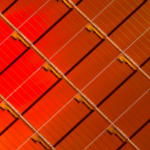
After construction, a conformal coating, a nonconductive protective layer, is placed to the PCB to shield it from atmospheric agents (Figure 1). This technique frequently used to PCBs for consumer, appliance, and mobile devices since they frequently function in environments with moisture, dust, or other abrasive elements. The protective layer that has been put to the PCB allows moisture in the layers to escape while keeping outside elements from getting close enough to the board to endanger its components’ functionality. The conformal coating increases the circuit’s lifespan in addition to dependability.

The most popular conformal coating materials are silicone, acrylic resin, polyurethane, and p-xylene, each of which can offer a particular degree of protection. For applications requiring high temperatures, silicone, for instance, is the ideal option since it can withstand a wide variety of temperatures. On the other hand, silicone is less chemically resistant than acrylic resin and has less adhesion to various substrate types. The latter is less suited in the presence of shocks and vibrations due to its hard construction. Polyurethanes are very resistant to moisture, abrasion, and vibration. They can handle low temperatures well, but not high ones. Thus, they are mostly employed in situations where the temperature ranges from -40°C to +120°C. P-xylene is a consistent polymer that provides excellent protection, but it is pricey and must be sprayed in a vacuum due to its sensitivity to impurities. There are four methods for applying the PCB conformal coating: dipping, automated selective coating, spraying, and brushing. All of these solutions accomplish the same thing, which is to completely cover the PCB, including the jagged edges and all board edges. Following application, the conformal coating is cured using UV radiation, air drying, or oven drying.
Elevated temperatures
The operating temperature will inevitably rise as component density on the PCB increases, which over time might jeopardise the integrity of the welds or the layers themselves owing to the expansion and contraction of materials with various physical qualities. Therefore, a dielectric having a glass transition temperature (Tg) of at least 170°C should be used in a high temperature PCB. As a general guideline, operating temperatures should be up to around 25°C below the Tg value of the material being employed. In addition to material selection, the high temperature of the PCB may be controlled by transferring heat from one part of the PCB to another. A heat sink that can remove heat from the hot component first via conduction (from the component to the heatsink) and then by convection can be put on it if it is mounted on the top side of the PCB and has a big enough surface (from the surfaces of the heatsink to the surrounding, colder air). Designers frequently employ the technique of inserting numerous thermal paths on the PCB to transfer heat away from the hot component to a layer of copper on the top of the PCB, where it can then be further transferred to a suitable heat sink, if the hot component is mounted on the underside of the PCB and mounting a heat sink is not possible. In order to enhance the dissipation area, PCB mounted heat sinks are typically big and have finned or corrugated surfaces. When compared to natural convection cooling, fans can be added to improve forced convection cooling. Using heavy copper technology is one of the conventional ways to combat the consequences of high temperatures. As a result of the lower resistance, heat losses are decreased, and the maximum current that the PCB traces can carry is increased.
Radiation protection measures
Using “rad-hard” components is the only solution for extended space missions. These parts are substantially more costly than regular parts since they are more rarer. Subject to examination and certification of their radiation resistance, the use of common commercial components may be permitted for brief space missions (up to one year). By doing so, you may increase the variety of design-able components and lower the cost of designing space equipment. Radiation impacts can be mitigated by using various hardware design methodologies. For instance, it’s crucial to guarantee that all metal pieces have sufficient grounding at the PCB design level.
Corrosion prevention and mechanical
The PCB can be put in a container and entirely encapsulated with epoxy to give protection against shock and vibration. The level of protection improves with increasing resin layer thickness. However, the resin layer’s thickness will vary across the board unless every component on the PCB has the same height, offering varying degrees of protection for every component. Therefore, in the worst situation, the amount of protection provided throughout the board corresponds to the thinnest resin layer. The PCB has to be properly cleaned before even thinking about resin encapsulation. Surface contamination, especially in situations of chemical resistance, might have a detrimental influence on the degrees of protection provided by encapsulation (as it provides an easier path for chemicals to enter). The weak layer creation between the resin and the PCB, which ultimately results in delamination, will also adversely damage the resin’s capacity to absorb thermal and physical shocks. The PCB is shielded against ionic pollution and corrosion by being kept dry and clean. Applying a conformal coating and using surface treatments like HASL and ENIG, which include dipping a PCB in an alloy of liquid lead and tin before levelling the alloy deposits with hot air jets, can both prevent corrosion (gold dipping). The detail of a PCB with an ENIG coating is shown in Figure 2.