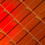
One of the most crucial stages toward a successful printed circuit board is choosing the substrate that is most suited for your electrical circuit. The substrate, which is the material used to create the layers that make up the PCB stackup, must possess electrical, physical, and mechanical properties that ensure the circuit will operate correctly under a variety of operating situations. The substrate, which is the insulating material located in the middle of the printed circuit board stackup, is shown in Figure 1 as the structure of a typical double layer PCB. The primary characteristics that affect substrate choice will be discussed in the following paragraphs, along with the selection criteria to be used and several real-world applications using datasheets for commercial substrates.

Thermal properties
Thermal conductivity (K), decomposition temperature (Td), glass transition temperature (Tg), and coefficient of thermal expansion are the four key thermal characteristics that influence the choice of a substrate (CTE). A material’s capacity to endure heat is indicated by its thermal conductivity, which is sometimes denoted by the symbol K. The Watt per meter Kelvin (W/mK) is the unit used to measure thermal conductivity. The most typical thermal conductivity ratings for dielectric materials are between 0.3 and 6 W/mK. In contrast, conductive materials are able to transport heat more quickly than dielectric ones because of their extremely high thermal conductivity (386 W/mK for copper, for instance). When the substrate is exposed to a temperature over a certain threshold on a printed circuit board, we can discuss decomposition. This temperature is known as the decomposition temperature and is denoted with the symbol Td. The reaction that happens, regardless of temperature value, is irreversible, making the degradation of the substrate a highly crucial process that must be strictly avoided. As a result, materials for PCB substrates must be chosen that can endure sufficiently high temperatures. A acceptable figure for Td may simply be 250°C given that the PCB is exposed to temperatures between 200°C and 250°C during the soldering process. The temperature at which the substance that makes up the substrate starts to soften is known as the glass transition temperature, or Tg. Due to the fact that this process is reversible, when the temperature falls below the Tg threshold, the substrate will harden and revert to its original condition. As a result, we may say that the substrate has the ability to change between rigid and glassy states, and that this transition is influenced by the value of Tg. We’ll examine what Tg values the most popular PCB substrate materials can have later. The material that makes up the PCB substrate’s rate of expansion is measured by the coefficient of thermal expansion, commonly known as CTE. The CTE value, which is expressed in parts per million, often increases when a substrate is subjected to temperatures over the Tg threshold (ppm). The CTE value rises in proportion to the substrate’s exposure temperature. However, the CTE value of the copper layers and the substrate varies from one another. In reality, copper has a lower CTE value than the substrate, which might lead to problems because of the differing expansions that the materials go through as the temperature rises. Materials having low CTE in both the X and Y axes of the PCB plane are often preferred. CTE typically ranges between 10 and 20 ppm; nevertheless, it must never exceed the maximum value of 70 ppm.
Electrical properties
Electrical strength, volume resistivity, surface resistivity, loss tangent (or dissipation factor), and relative permittivity are the primary electrical parameters that need to be taken into account while choosing the right substrate (also known as dielectric constant). The electrical strength, expressed in Volts/mil (1 mil=0.001 inch), shows the capacity of a dielectric material to withstand an electrical defect and is measured along the vertical direction (Z axis) of the printed circuit board. The majority of the materials used to make substrates have electrical strengths ranging from 800 to 1500 V/mil. The Greek letter stands for volume resistivity, which represents a dielectric material’s resistance to insulation or electricity. High resistivity substrate materials will be less likely to promote the start of electrical charges. Therefore, these materials must possess a high resistivity, preferably between 103 and 1010 M/cm, like other dielectric insulators. External variables like heat, cold, and humidity have an impact on the volume resistivity’s value. A dielectric material’s surface resistance to insulation and electricity is expressed by its surface resistivity, denoted by the symbol S. Similar to what is done for the volume resistivity, a high value for S, preferably between 103 and 109 M/cm2, must be selected. Additionally, the high values of temperature and humidity have a general impact on even the value of S. The ability of the material to distribute power is expressed by the dielectric loss tangent, often known as the dissipation factor (usually denoted by the terms Df or tan). In any event, the dielectric loss tangent (tan) of the materials used as substrates in printed circuit boards is a function of the frequency of the signals that pass down the PCB traces and typically falls between 0.02 and 0.001. The electrical behavior of the printed circuit board is significantly influenced by the dielectric constant or relative permittivity, denoted, respectively, by the parameters r and Dk. The dielectric constant is a function of frequency; specifically, it decreases as the frequency rises. Its value typically ranges from 3.5 to 5.5 (depending on the individual material). It is essential to pick materials with a dielectric constant that is stable across a broad frequency range when working with high frequency transmissions.
Guidelines for substrate selection
Some design decisions that might be crucial to a printed circuit board’s success must be made in the early phases of the PCB’s creation. These options include picking a material that will satisfy the functionality and dependability standards set for the printed circuit board. The following is a summary of the most typical factors used to choose the best material for the substrate.
1 – Match the values of the dielectric constant
There are materials with various dielectric constant values in every printed circuit board (Dk). If these values are not correctly matched to one another, issues may occur (for example, if these values differ substantially).
2 – Match the coefficient of thermal expansion
The coefficient of thermal expansion (CTE) is perhaps the most significant of a substrate’s several thermal characteristics. A suitable matching must be established for the CTE, just as it is done for the dielectric constant Dk. In order for two substrates to be compatible, their CTEs must match. Otherwise, the PCB might change or have flaws because the two substrates could expand throughout the manufacturing process at extremely different speeds and amplitudes.
3 – Use a tight weave for the substrate
The diverse materials may be made to interact appropriately by weaving a substrate with an extremely tight weave. In instance, a highly tight substrate weave will have a relatively uniform distribution of the dielectric constant Dk.
4 – Avoid using FR-4 in high frequency applications
Due to its low cost and ease of availability, the FR-4 (Flame Retardant Level 4) material is frequently used in many non-critical applications, however it is inappropriate for RF applications, particularly those where high frequency signals are present. In actuality, the FR-4 has a substantial dielectric loss.
5 – Use only materials with low moisture absorption
The ability of a substrate material to withstand water absorption while submerged in an aqueous solution is expressed as moisture absorption. This index is calculated using a conventional test procedure and the percentage weight gain that the material experiences after absorbing water. The materials utilized as substrates typically have moisture absorption values in the range of 0.01% to 0.20%.
6 – Use CAF resistant materials
Conductive anodic filament, or CAF, is a metal filament that can seriously and permanently harm the printed circuit board. It is created by an electrochemical migration process. Such harm can range from dielectric breakdown between the conductors of the printed circuit board to current leakage and sporadic electrical short circuits. The danger of CAF must be reduced by choosing materials that give good resistance to this phenomena because it is a very sneaky problem that is difficult to identify with normal monitoring equipment.
A practical example
Consider the datasheet for a substrate material of commercial grade, such as the Rogers Corporation’s RO4000, as an illustration. This material, which is especially well suited for high frequency circuits, has extremely little dielectric loss and can be produced using the same conventional procedures as FR-4. This material ensures excellent performance across a wide frequency range by maintaining the dielectric constant practically constant as the frequency changes. The RO4000 material exhibits exceptional dimensional stability due to the coefficient of thermal expansion (CTE) taking values that are extremely comparable to those of copper. The expansion of the substrate is guaranteed to be steady across the whole range of working temperatures when Tg is greater than 280°C. The RO4000 datasheet is partially depicted in Figure 2. The values of the key thermal and electrical characteristics, including Td, Tg, CTE, tan, and more, may be found here.