Electronic technology has made great strides in recent years, opening up new uses and scenarios that were previously critical or impractical. Printed circuit boards are currently needed for high-performance technologies with ever-increasing complexity and criticality, including 5G mobile networks, connected and autonomous vehicles, data centers, Internet of Things (IoT), aerospace, and military applications. With regards to things like power stability, signal integrity, thermal management, ultra-high frequency digital signal management, circuits with mixed analog and digital signals, and more, electronic designers face more difficult technical hurdles.
Examples of critical applications
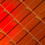
Printed circuit boards are used in the most crucial applications in the avionics, aerospace, and defense industries. Even though these PCBs are produced in far lesser quantities than goods of a commercial grade, there are much higher expectations for their performance. Critical applications require more development time and have a significantly longer projected life, often between 5 and 15 years, whereas the accepted technology in commercial goods is thought to become obsolete after an estimated duration of 2–5 years. These PCBs must meet all applicable standards, including DFT (Design for Test), New Product Introduction (NPI), and DFM, and they must have 0% fault tolerance as well as go through rigorous testing processes before being manufactured (Design for Manufacturability). It is best practice to design the circuits to withstand currents with higher than rated currents to ensure that the circuit is not damaged under difficult operating conditions. PCBs developed for critical applications frequently require components with tighter tolerances (1-2%) than commercial grade components (5-10%). We are all aware that designers are taking use of printed circuit boards’ performance more and more. The printed circuit board continually experiences high temperatures due to the rising power density. Such temperatures might result in unpredictable system operation or even breakdown. Particularly if the boards are subjected to cyclical heating and cooling, the variations in the thermal expansion coefficients of the materials that make up the PCB can also result in mechanical strains, which can shatter the circuit and cause problems with the electrical connections. The Tg index, which is the temperature range in which the substrate material goes from the solid, stiff, or glassy state to the rubbery state, is best used when the temperatures created on the printed circuit are high. The choice of materials having a Tg index at least 20–25°C higher than the anticipated operating temperature for the device for which the PCB is utilized is a typical practice among designers. For instance, if the board has a Tg value of 130°C, the device’s operating temperature should never go over 110°C. A PCB with high Tg materials (Tg=180°C in this example) is detailed in Figure 1.

Heavy copper and other unique construction methods, which can increase the current carrying capacity by lowering power losses, are used in PCBs made at high temperatures. While employing the same manufacturing method as conventional boards, with the exception of unique etching and plating procedures, the copper layers in this case are thicker and heavier than standard PCBs. Similar method, known as “copper coin,” involves directly inserting copper plates (either circular or not) onto the printed circuit board (PCB) at the locations with the highest heat concentration. Due to the heat sinks being built into the board and not requiring external cooling systems, this also results in cost savings.
Design guidelines
We will now go through the key principles that designers may adhere to to make PCB creation for crucial applications simpler and more successful.
1 – Layout
There are several precautions that the designer can adopt when defining the layout. The main ones are the following:
- In order to limit noise and prevent harmful couplings between signals put on neighboring traces, the length of traces carrying high-speed signals (such as clock signals) should be kept to a minimum. To prevent unintended energy transfers between the board and the outside world, the traces attached to the connection I/O pins should also be as short as feasible.
- In order to prevent potential inductive or capacitive interaction with the power devices, high frequency signals should never be routed below them. Always place clocks and any other crucial signals on layers close to the ground or power planes.
- In order to avoid connectors from acting as an antenna, connectors should be positioned on the same layer (or, better yet, on the same side) of the board. This will reduce the common mode voltage that might be created between their I/O pins.
- In order to restrict the strength of the electric and magnetic fields produced by these traces, which might also cause crosstalk with signals put on other layers, high-speed signal traces shouldn’t be positioned too close to the board’s edges. The differential signal-related traces must always be paired and separated by the same amount.
- In order to prevent the creation of short circuits, electric arcs, or high frequency couplings, power planes should be properly separated from one another (for instance, with a minimum spacing of 3 mm). Connections between power and ground planes on a PCB stackup should never be established with traces; instead, they should be made with vias that are close to the component’s power or ground pad. Each link from one point in the circuit to ground should extend to all ground planes if the stackup has multiple ground planes. When high frequency signals are present, the current has a tendency to select the route with the lowest inductance. Consequently, the current may be prevented from picking the optimal route by connecting to only portion of the ground planes.
- Ground planes should always be uniform (that is, solid) and have no gaps, thus creating a grounding path for the current.
2 – Stackup
Impedance control requires the use of power planes, which are situated beneath the signal layers and are capable of offering a current return path. In the PCB stackup, these planes should be distributed uniformly, making sure that there is a layer next to each signal layer that supports impedance control.
It is vital to choose the qualities of the substance that makes up each layer in addition to the suitable arrangement of the ground and signal layers, such as:
- Copper thickness
- Dielectric thickness
- Dielectric constant
Utilizing components with high dielectric constant and low loss tangent improves power integrity and reduces signal losses, making them ideal for stackup.
3 – Impedance control
Signal integrity issues are being created by the steadily increasing switching speed of signals moving across the PCB. The traces on a printed circuit board may therefore no longer be thought of as straightforward point-to-point connections, but rather as actual transmission lines that need the proper impedance matching to guarantee good signal integrity. Building traces with a relatively uniform cross-section shape is required since the maximum strength of a signal that travels down a PCB trace can only be reached with an acceptable impedance matching. The smoother the dielectric constant is along the whole trace, the more uniform the trace is, and the less power degradation it experiences. Neglecting impedance matching can lead to harmful signal reflections, which impair circuit energy efficiency and cause power losses. With knowledge of each trace’s length, as well as other factors like the substrate material’s dielectric constant (Dk), values for each trace’s width and thickness may be calculated using appropriate software tools (also known as impedance calculators), some of which are readily accessible online.
4 – Crosstalk
Due to the latest generation of printed circuit boards’ high density, crosstalk, also known as undesired electromagnetic field coupling, is a possibility due to the PCB traces’ near proximity to one another. Crosstalk happens when a signal that is sent on one trace causes undesirable effects (signal spikes or oscillations) on the lines that are nearby. The length of the portion where the traces are parallel to one another determines how much crosstalk occurs. The amount of crosstalk increases as this segment becomes longer. The most typical recommendation for reducing crosstalk is to keep traces at least three times wider apart than the width of the trace itself, as illustrated in Figure 2. The separation between the traces in differential signal pairs must be at least five times the trace width (5W rule).

Signals are often routed on two neighboring layers of a multilayer PCB. When this occurs, we must ensure that the traces on each layer are parallel to those on the layer next to it. Through this configuration, parallelism between the traces is avoided, and crosstalk is reduced.
5 – Components placement
Another important element in making a printed circuit board appropriate for high-critical applications is component location. The first way to categorize components is according to their functionality, or if they carry out the same or comparable tasks. To reduce potential electromagnetic interference, analog components, for instance, should be located apart from digital components and lines. In order to enhance impedance matching, the components that produce high-speed signals should be positioned on traces with as little room between them as feasible. Additionally, these parts shouldn’t be put close to board edges or sources of interference like switching power converters. When the PCB is relatively compact in size, component placement might turn into a very challenging problem.