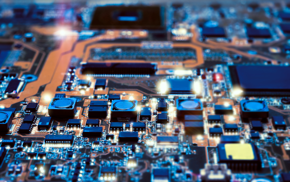
For electro medical applications, printed circuit boards now hold a vital position. The deployment of medical devices with increasingly sophisticated features, such as pacemakers, defibrillators, cardiac monitors for the treatment of cardiovascular diseases, diagnostic imaging, magnetic resonance, CT, and ultrasound equipment, as well as a wide range of portable and wearable solutions, such as thermometers, blood glucose monitors, and electrical muscle stimulation equipment, has been made possible by the significant advancements made in the field of electronic technologies. Medical grade PCBs must be safe for patients and healthcare professionals, conform with appropriate safety requirements, and have great dependability and durability in order to keep up with these developments.
Technologies for PCBs in medicine
The present trend in electro-medical device development is toward ever-smaller products with an ever-greater component density, just as it has already occurred in other electronics sectors. The arrangement of the components and their relative distances, the length and spacing of the traces, and the PCB’s ability to dissipate heat are just a few effects that are unavoidably affected by this. As a result, the margins of error in a board’s design have substantially shrunk, thus necessitating more flexibility throughout both the design and production phases. The PCB technology that enables the construction of high-density connection boards is one that can meet this demand (HDI). The space available for routing the traces, which are getting closer together, is therefore reduced by lowering the size of the PCB and increasing the quantity and complexity of the implemented functionality.
Flex and stiff flex printed circuit boards are based on another technology that is frequently utilised in medical PCBs. This is due to the fact that medical devices frequently deviate from the standard size and shape of conventional PCBs and must be able to squeeze into the smallest space while maintaining the same levels of dependability and durability. Since flexible PCBs are constructed of lightweight components, the gadget as a whole weighs less. These PCBs’ flexibility enables for the optimization of space and production costs, giving the designer more latitude to choose the case’s shape. Although a flexible PCB’s design is more intricate than a rigid one, it is considerably simpler to create a durable and ergonomic gadget. In reality, flexible PCBs outperform stiff PCBs mechanically in a wide range of medical applications, particularly wearable ones. Additionally, flexible PCBs may connect to stiff boards using short, flat wires rather than big, tall connections.
The development of devices with non-standard PCB form factors, such circular or elliptical, is being driven by the present trend of numerous wearable gadgets, such as those which monitor vital signs for training, fitness, or therapeutic purposes. The PCB can occasionally assume wholly atypical forms. Designers can manage even the most dissimilar types of printed circuit boards with ease thanks to the integration of rigid-flexible and flexible-flexible PCBs (which are very small and have a high component density). An illustration of a rigid-flexible PCB is shown in Figure 1.

The following paragraphs will give a few straightforward guidelines that can assist designers in creating medical PCBs by making the process of designing, testing, and maintaining them easier.
1 – Components with SMD and PTH
Although plated-through-hole (PTH) mounting technology may be more appropriate for some devices, surface mount technology (SMT) has become the de facto standard for the majority of electronic applications. This is especially true for power supply boards and situations where multiple connectors are used. SMT technology is often used for medical applications because it enables the use of smaller components, which reduces the size of the PCB and increases component density on the board. Additionally, since no holes need to be drilled when assembling SMD components, fabricating and assembling the printed circuit board takes less time and money. The 008004, seen in Figure 2, is one of the tiniest SMD packages currently on the market and measures just 0.25mm x 0.125mm.

2 – Materials
The selection of materials used for PCB fabrication is especially important because of the importance of medical equipment, whose safe and dependable operation frequently depends on the lives of many patients. The following are the primary variables that influence the selection of materials and substrates best suited for a certain medical application:
- adherence to RoHS guidelines;
- RF signal availability and/or high frequency/transmission speed signal availability;
- maximum operating temperature;
- connection choices (WiFi, Bluetooth, etc.);
- case size and form.
The usage of HDI technology is common, leading to a high number of interconnections and via holes, both blind and buried, in order to accommodate the high density of components required. As a result of the ability to create via-holes using a laser, as well as via-in-pads and tracks with a width and spacing of only 5 mil, HDI technology enables a significant reduction in PCB footprint.
The via-in-pad technology enables holes to be made directly on the pads, connecting the pads to the internal layers and is typically used with highly integrated components (like BGAs) or with a high number of pins and a very tight pitch. A via-in-pad technology application is shown in Figure 3 with via holes put directly on some component pads.

The fabrication of HDI PCBs for medical applications does, however, necessitate the purchase of pricey machinery, including direct laser imaging (LDI) and additive and semi-additive processes (mSAP), which raises the PCB’s manufacturing cost. To achieve the exacting standards for trace width and spacing, such equipment is required. Due to its affordability and relatively simple manufacturing, FR-4 (Flame Retardant Level 4) is another laminate material that is frequently chosen for medical PCBs. The PCB may need specific laminates like polyamide, Teflon, PTFE, or ceramic-type materials in the case of more complex machinery or for devices falling under higher danger classifications. Particularly suited for all high frequency electronic applications are these materials. In these situations, the FR-4 material’s dielectric constant, which is roughly equivalent to around 4.5, proves to be excessively high, leading to considerable signal losses during transmission via the printed circuit board. On the other hand, materials with dielectric constants of 3.5 or less include Teflon. These materials not only have a lower dielectric constant but also have outstanding thermal properties, with Tg values up to 280 °C.
3 – Longevity
It is crucial that designers, working with suppliers and PCB manufacturers, have the ability to foresee component obsolescence throughout the design process of a medical PCB. What we need to prevent is the project’s early closure due to the inability to locate specific components. If this occurs and the necessary alteration at the component or schematic level is sufficiently important, the product may need to go through the approval procedure again in order to get the necessary conformities (approval by the competent organisations may take several months).
4 – Maintenance
The goal of PCB design at every stage must be simple assembly and upkeep. Evidently, this has an impact on a number of factors, including trace routing, PCB layout, and component placement.
The connectors require special care to ensure that installers and maintenance staff can access them without difficulty. Any of the pads must be positioned and sized to make the soldering process easier, and all integrated components with many pins must be correctly aligned. Additionally, a height profile that is as uniform as feasible must be maintained on the PCB, isolating the components with larger height from the others. The creation of a 3D model of the complete circuit is also advised, and many PCB construction programmes can now execute this task nearly automatically. This model enables the designer to assess the board’s overall and real dimensions, offering crucial recommendations for the assembly and installation process within the case.
5 – Test and fix
The complete board has to be created in a way that makes it easier to test and troubleshoot the circuit. Enough test points must be included by designers in order to simplify the diagnostic procedure, both in the factory and on the job. Test points should primarily be put on the power lines, the clock and control signals, and the signal traces transporting signals. Experience has taught us that it is always preferable to have a few extra test points than to have someone missing at the circuit’s most crucial junctions. Additionally, it is always preferable to position test points on the board’s outer sides. The test and verification step will be considerably simpler once the printed circuit board has been put together and fitted in the housing.
6 – Simulation
The design of medical-grade PCBs can benefit greatly from simulation approaches like Digital Twin, which lower development costs and speed up time to market. Simulation’s key benefit is that it aids in spotting potential errors before delivering the initial board prototype. By using data from the actual world as input and simulating or predicting how the circuit will react in response to applying those input stimuli, digital twin technology effectively builds a virtual model of the circuit. This enables data analysis and system monitoring, allowing engineers to identify possible problems before they arise, gauge the amount of downtime, and enhance the functionality of the product. The circuit’s thermal modelling, which enables the early detection of potential hot spots when the circuit is operating under various load and environmental circumstances, is also crucial. If changes to the circuit are necessary to meet the reliability and safety requirements imposed by the applicable standards, it is always preferable to spend a few hours changing the schematic and running the thermal simulation again rather than performing an expensive thermal analysis with infrared cameras on the finished product.


