As the market for electric vehicles grows daily, so does the demand for reliable power electronic systems for processing and converting electric energy. There will be a shortage of the semiconductors on which we currently rely in the coming years. The need for smaller, more energy-efficient devices has increased over the last few years. Wide-Bandgap semiconductor research is expanding as a result of the numerous limitations that traditional semiconductors face in terms of their ability to effectively perform the circuit.
Technologies based on Wide-Bandgap semiconductors are meeting all of the industry’s needs today. They have a larger bandgap, as the name implies, which allows various electronic devices to operate at high voltages, temperatures, and frequencies. Silicon Carbide (SiC) and Gallium Nitride (GaN) are two recently introduced wide-bandgap semiconductors with higher power efficiency, smaller size and weight, and lower overall cost. Silicon-based devices have multiple limitations, due to which SiC and GaN can be ideal replacements for them.
Why are Gallium Nitride (GaN) and Silicon Carbide (SiC) used?
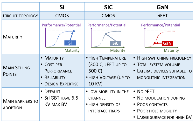
SiC has demonstrated the ability to produce more power, which has proven to be very valuable in the field of electric vehicles (EVs) and can therefore be broadly used for industrial automation. GaN has a higher switching frequency and uses less energy. Apart from this, GaN also has greater electron mobility than silicon, allowing electrons to flow more swiftly across semiconductors.
A description of the properties and characteristics of wide-bandgap materials
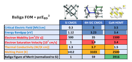
Wide-bandgap materials have a 3 eV+ wide-bandgap, which makes it a crucial characteristic for carrying out high-voltage activities. In a Field-Effect Transistor’s 2D channel, mobility and saturation velocity are suited for high switching frequency (FET). However, the lower mobility of SiC with interface remains to be one of the limitations of these SiC requirements. GaN’s high density of 2D electron gas and its piezoelectric properties for interfacing and modulation doping enable 2D mobility. GaN FETs have a wide range of benefits, which include greater operating frequencies, improved thermal conductivity, a higher melting point, and more.
Maturity in Applications of Wide-Bandgap Technologies
The figures of merit provide a summary of the fundamental characteristics of the WBG materials (FOM). The analysis of innovative semiconductor devices made after 2015, such as Silicon super junction MOSFETs, SiC MOSFETs, and GaN FETs, is highly helpful for assessing the maturity of the devices and identifying areas that require development. The Baliga FOM, for instance, records the characteristics relating to high voltage operations and resistive power losses (BFOM). This is a 1D electrostatics-based unipolar device’s normalized breakdown voltage at on-state resistance parity. The operation of unipolar devices like MOSFETs and High-Electron Mobility Transistors depends on BFOM, which relates to carrier mobility and is proportional to it (HEMTs).
Wide-bandgap Field Effect Transistors (FETs)
SiC MOSFETs come in two different shapes, notably –
- Planar
- Trench

Low mobility due to high contact trap density restricts the Ron. Ron is on-resistance, which implies it is the resistance present between a MOSFET’s source and drain. Ron’s value must be low to indicate that there is little power loss. SiC MOSFETs have a breakdown voltage of 15 kV and a range of 1.2 kV to 6.5 kV. Since the Ron is too high to use the SiC MOSFET for application applications, the issue can be practically rectified by increasing channel mobility.
Considering the Benefits and Drawbacks of Silicon (Si), Silicon Carbide (SiC), and Gallium Nitride (GaN)
Limitations in Using GaN
Despite its numerous advantages, using GaN has some reliability-related limitations. These limitations will be eliminated with advancements in GaN fabrication technology.
Some of the limitations are as follows:
- Degradation in dynamic resistance: High drain voltage and current during high switching operation on GaN result in the semi-ON situation, which has an effect on the circuit’s performance. The result is the trapping of a negative charge. As per previous experiments, it could be seen that degradation is caused by the combined action of charge trapping at the surface and in the buffer layer.

2. pGaN HFET threshold voltage instability: This is a serious issue in pGaN HFETs. The nature of the ohmic gate determines the threshold voltage’s instability.
Potential Markets for SiC and GaN
Despite its growing market reach, Wide-bandgap semiconductors can be used in only specific applications. GaN devices today make up a total of 0.1% of the world’s semiconductor market. Future market forecasts state that in the following five years, the yearly growth rate will rise by 35% to 75%. The low-end sector, along with consumer goods like quick chargers, screens, and data centers, can drive the majority of the revenue.
Additionally, SiC inverters for PV systems, GaN and SiC rectifiers, and DC/DC converters for ultra-fast chargers for electric vehicles can all be made with WBG Semiconductors. GaN and SiC have the ability to improve power electronics’ performance and generate outputs that are more efficient than those produced by conventional silicon devices. Compared to silicon-based devices, there is a lot more room for development, given the constraints of WBG SiC and GaN. Only when the technology is improved can the needed improvements be made. Furthermore, WBG materials are less expensive than conventional MOSFETs in the market today. WBG semiconductors will create an industry with a rapid potential increase in its production. This can be used as an alternative to the existing silicon-made devices, as restrictions of SiC and GaN MOSFETs will get eliminated, creating new advantages.


